http://www.cypress.com/knowledge-base-article/interfacing-sram-jtag-signals-using-voltage-level-shifter-kba81536
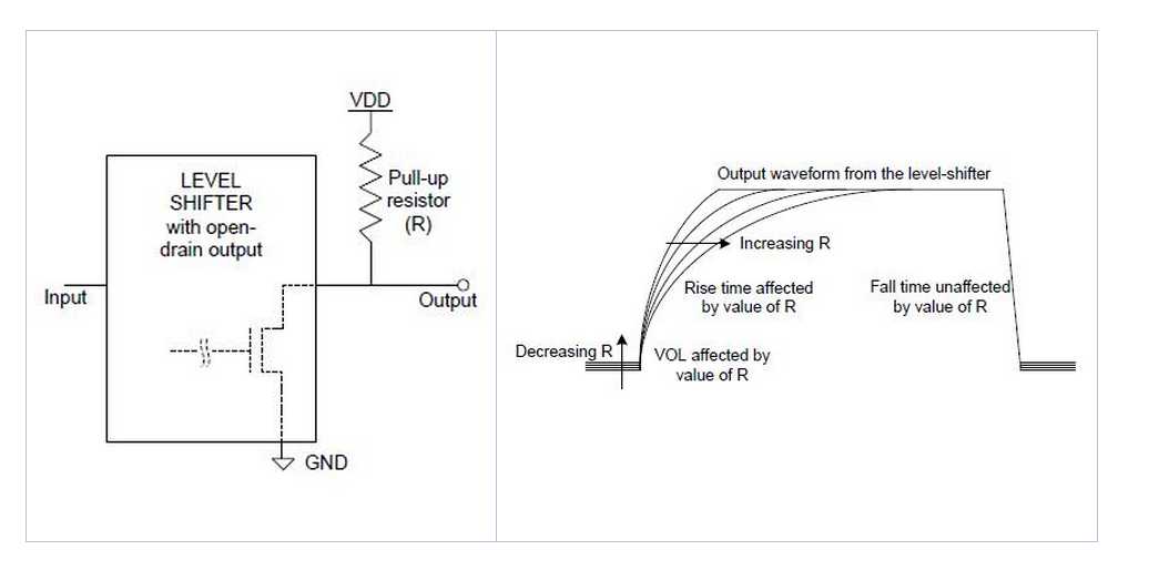
As a best practice, avoid use of level-shifting ICs with open-drain output.
This type of level-shifter requires a resistive pull-up to achieve output high voltage (VOH).
The slew rate of signal from level-shifting IC going to the memory device depends on the value of the pull-up resistor;
the higher the resistor value, the lower the slew rate and vice-versa.
Figure 2 shows the output waveform from this type of level-shifter.
Figure 2: Effect of Pull-up Resistor on Signal Rise Time for Level-Shifter IC with Open Drain Output
If the open-drain output level-shifting IC is already built into the system,
the problem of false clock/signal trigger can be mitigated by use of a smaller resistor value
at the expense of a slightly higher VOL signal from the level-shifting IC.
Identification of the optimal value requires experimentation with various pull-up resistor values.
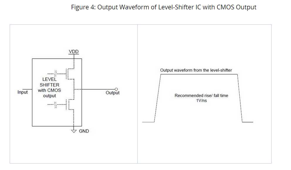
Cypress recommends the use of level-shifting ICs that provide CMOS rail-to-rail output.
This produces a strongly driven VOH/ VOL signal from the level-shifting IC to and from the memory device.
We also recommend maintaining the signal rise and fall time equal to or better than 1 V/ns.
Figure 4 shows the output waveform for this type of level-shifter.
Voltage Level-Shifter Output Waveform
原文:http://www.cnblogs.com/shangdawei/p/4820615.html