http://www.serasidis.gr/circuits/RFID_reader/125kHz_RFID_reader.htm
http://www.serasidis.gr/circuits/RFID_reader/images/125kHz_RFID_reader_schem.GIF

I will try to explain with simple words how the RFID works. The ATtiny13 uses the PWM function to produce an 125 kHzsquare wave signal. This signal comes out from PB0 pin. On the falling edge of the PB0 (Logic ‘0‘), the T1 does not conduct. So the L1 is energized from R1 (100 ohm) with +5V. When PB0 pin rises (Logic ‘1‘) the T1 conducts and one side of L1 goes to GND. The L1 goes in parallel with C2 creating an LC oscillator. These transitions of L1 to logic ‘1‘ and logic ‘0‘ are made 125000 times in one second (125 kHz).
Data communication between Tag and reader.
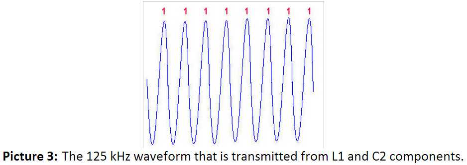
How an RFID Tag communicates with the reader? The idea is simple, but very clever! When a Tag wants to send a logic ‘0‘ to the reader it puts a "load" to its power supply line to request more power from the reader. That will make a small voltage drop on the RFID reader side. That voltage level is logic ‘0‘ (picture 4). Simultaneously, as long as the reader transmits the 125 kHz signal it reads the voltage of the transmitted signal trough the filters D1, C3 and R5, C1. When the Tag drops the voltage as we said before, the reader reads this voltage drop as logic ‘0‘. When the Tag doesn‘t require any additional power, it doesn‘t make a voltage drop. That is logic ‘1‘ (picture 3). The ‘Ones‘ or ‘Zeros‘ length depends on the serial transmission data rate. For example, for 125 kHz carrier frequency we don‘t have 125000 bits per second data transmission! The data transmission from Tag to the reader varies from 500 bits per second up to 8000 bits per second.

The RFID tag content EM4100
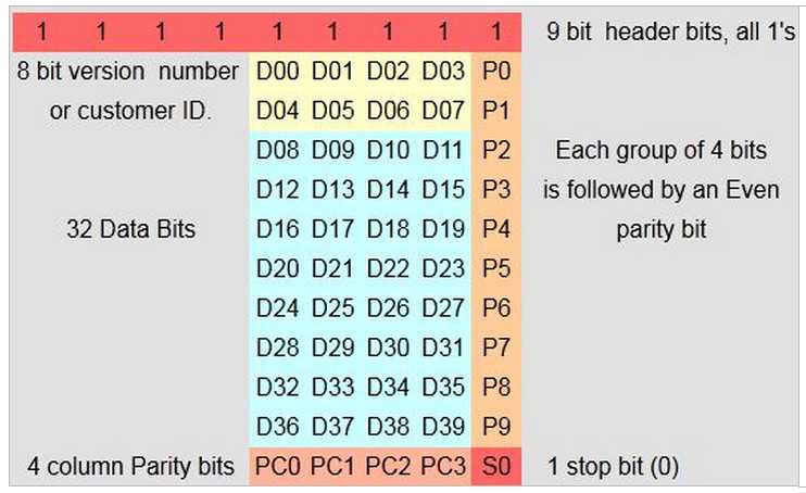
The 125kHz RFID tag transmits 64 bits.
The data verification is been done from ATtiny13 by calculating the Even parity bit of each line and each column with the parity bits that had been received form the RFID Tag transmitted data.

http://freshengineer.com/blog/simple-rfid-reader-module-design/
I first started by creating a simple, non-filtered, non-processed reader.
I’ve used a coil of about 1mH for both sides.
Since my chosen frequency was 125 KHz, my capacitor should be 1.62nF according to the following equation; I picked 1n5 standard value.

So this configuration is probably one of the simplest forms of an RFID reader-tag pair:
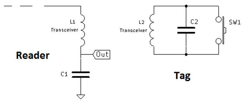
L1 is driven via a low-impedance 125 KHz oscillator, can be a sine or a square wave
since the LC circuit will filter out the unwanted harmonics that are presented in a square wave.
If the Q of the inductor is high, then a voltage that is greater than the oscillator’s output is going to be present in the “Out”.
I’ve seen 100 Vpp when I fed the LC circuit with 5Vpp!
So, the “Out” waveform at the top of the C1 is a sine wave of a 125 KHz frequency.
Now, the fun thing begins when we put the tag near the reader.
L2, C2 pair picks up the 125KHz waveform via L2. So, if you scope C2, you will see 125 KHz sine wave.
Now, if you scope “Out”, you will see that Vpp at C1 will drop when we close the switch SW1.
That is because we load L1′s magnetic field via L2.
Now, push the button like you are sending a Morse code and watch the “Output” waveform on the scope. Aha, modulation!
Simple! That is how real RFID passive tags work.
However, instead of sending Morse code, they modulate the signal with their specific modulation scheme.
I am going to work with EM4100 protocol since it is widely used.
Okay, let’s bring some real circuitry here.
http://freshengineer.com/Documents/RFID_Reader/KiCad/Outputs/Schematic.pdf
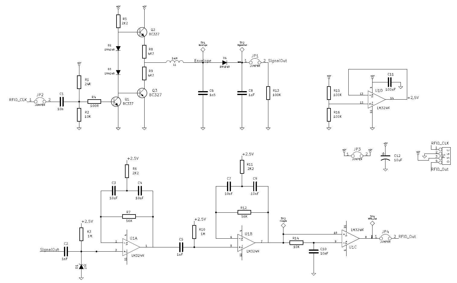
OK, L1 and C6 are our main guys.
They are the components that are mentioned before as “L1″ and “C1″ in Figure 1.
The circuitry on the left side of L1 is used to drive this LC circuit, and right side of C6 is used to read the changes in the signal.
C1 AC couples the clock signal of 125KHz to the circuit.
R1 and R2 biases the transistor Q1.
R4 limits its base current.
Q1 drives the input of push-pull follower formed by Q2 and Q3.
A push-pull follower will drive the signal at low output impedance.
D2 and D3 prevents distortions at the cross-overs from zero level.
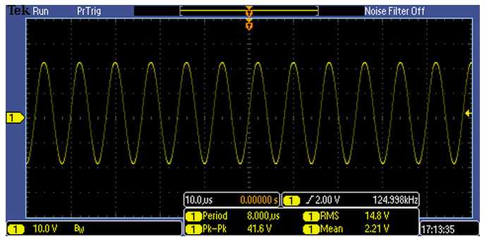
Now, our signal at “TP1″ is something like this, with no processing and modulation:
We are going to use an “envelope detector” formed by D4, C8 and R13.
After the recovery, this is how our “modulated” signal looks like:
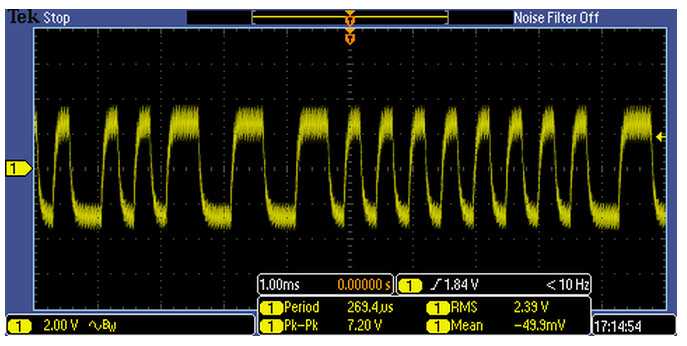
Of course, these measurements are made with the tag almost touching the reader.
If we move the tag away about 5 cm from the reader, we may not be able to see the signal even with the oscilloscope.
So, we have to filter and amplify this signal and make it ready to be processed by a microcontroller later on.
As you can see above, the signal we are dealing with is an AC signal.
To deal with AC signals with the OP-AMPs, you need either a dual supply which goes to negative (for example -12V, +12V),
or you need a virtual ground.
We are going to assume that half point of our supply voltage is ground.
So, if we are using a 5V single supply, our half point is +2.5V. If +2.5V is ground, then +5V is our new +2.5V and 0V is our new -2.5V.
There you have it, a dual supply.
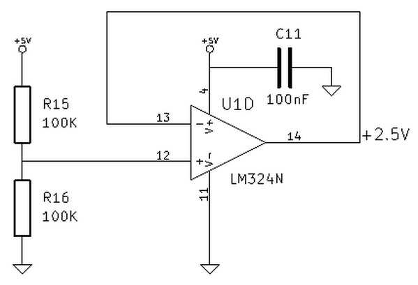
We need the output impedance of this supply low, so we use an OP-AMP to buffer the +2.5V point
which is high impedance due to R15 and R16, and we get a low impedance output as shown:
OK, now that we have solved that problem, let’s go back to our filter design.
We have a square wave at certain frequency that we want to boost.
While boosting the desired frequency we want to kill the other frequencies.
But we see a bump there; square wave.
A square wave is a signal that includes lots of harmonics (theoretically; infinity) of its actual frequency.
These harmonics are hidden in the rise and fall waves, sharper the rise and fall, more the harmonics count.
So, that means, if you low pass filter a square wave -that is not letting higher frequencies to pass a filter,
you delete those harmonics and remember, those harmonics are in rise and fall times.
Thus, you end up with a sine wave.
We do not want that, that’s why we are going to let these frequencies pass as the way they are, however we are going to boost the original frequency.
To do this, we have a filter design like follows:
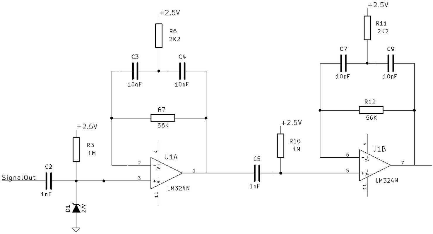
“SignalOut” is our input coming from the envelope detector.
C2 and R3 form a high pass filter to AC couple the input, and D1 protects the non-inverting input of the U1:A from over-voltage.
You may say that it is not needed as the capacitor C2 will not allow any DC voltage through, you are correct.
But only in steady state, if the capacitor is discharged, then it will let DC until it is charged.
By the way, think +2.5V point as a “ground” point, since it is a virtual ground.
C5 and R10 AC couples the output from U1:A in case of any DC offset.
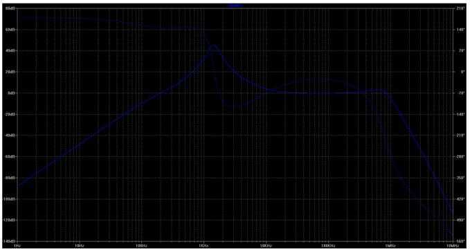
Then, this signal is filtered again, resulting in more amplification.
Here is a graph showing the transfer characteristics of these filters:
Here is the waveform at the output node, pin 7 of U1:
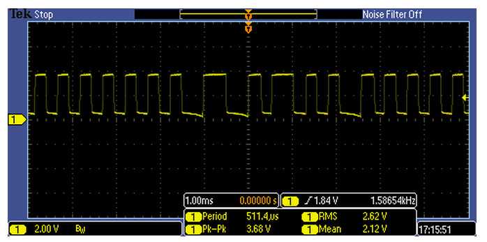
Yay! We have a filtered, clean output!
But not so fast, because we need logic output.
This is done easily by a comparator.
Normally, OP-AMP comparators compare the input with a reference voltage, generally half the supply voltage.
However, this may not work well if the rise and fall times of the input waveform is not in symmetry or close enough.
Let’s demonstrate that with a reference voltage of half the supply:
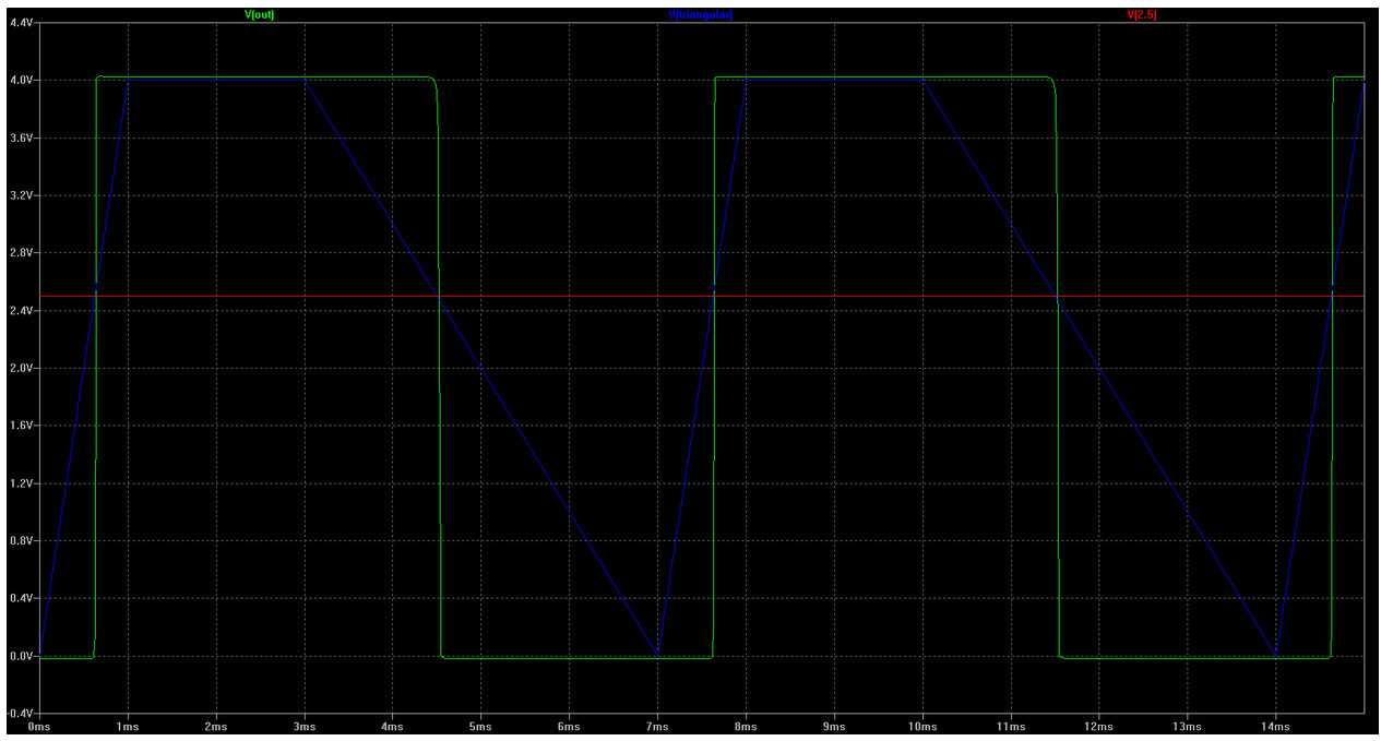
The input signal has a loooong fall time.
It should fall down at 3ms point ideally, since this is a recovered, however badly distorted ~43% duty cycle square wave - well at least let’s assume.
See how the output waveform is a ~56% duty cycle square wave. We do not want that.
What you have to do is simple, compare the input signal with its average.
How do you find a signals average? That is simple too - put it into a low pass filter, and here is the output:
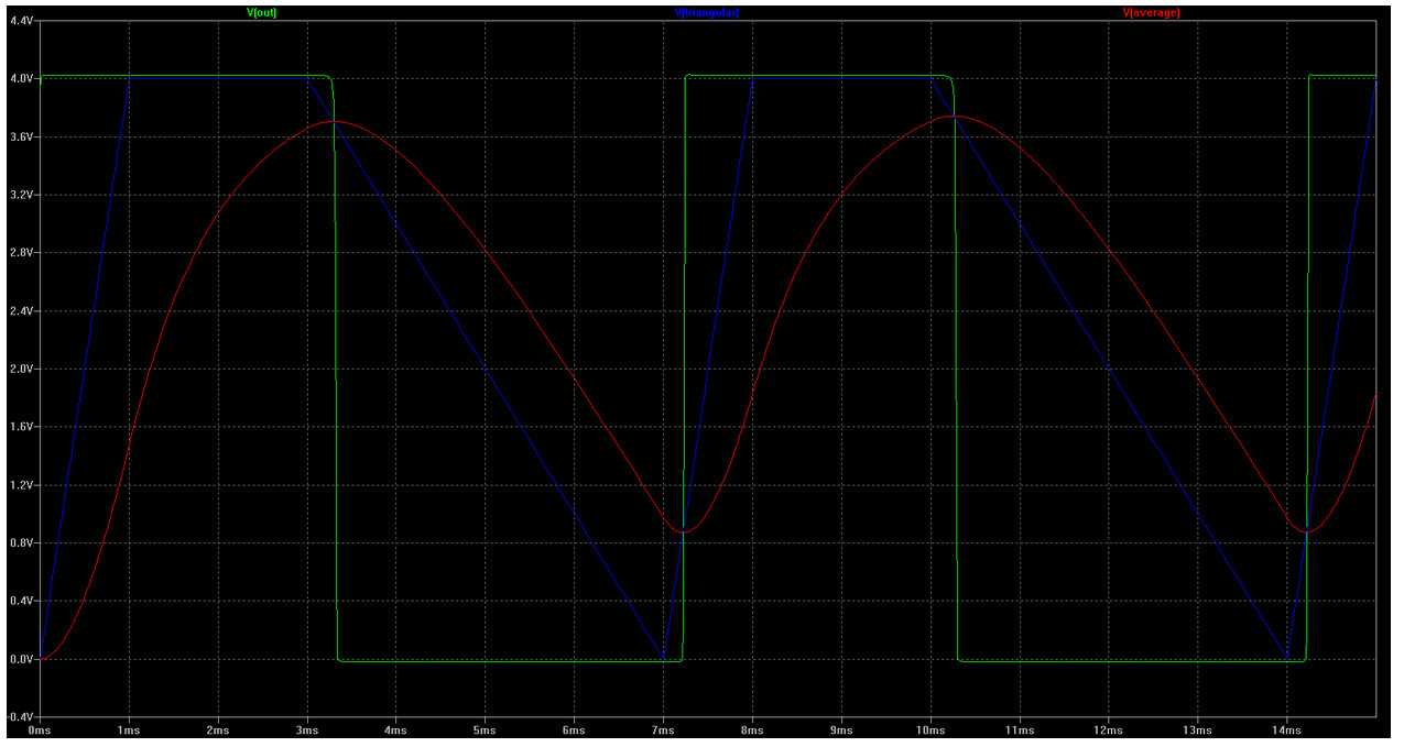
Now let’s look at our case and apply:
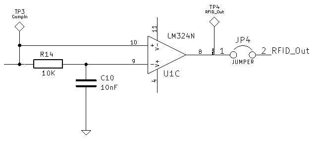
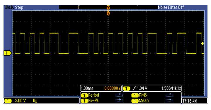
Let’s look at R14 and C10, we have selected them so that we have a good averaging (should I say weighted?) level for both 1KHz and 2KHz outputs we will have.
This is the final output, isn’t it great:
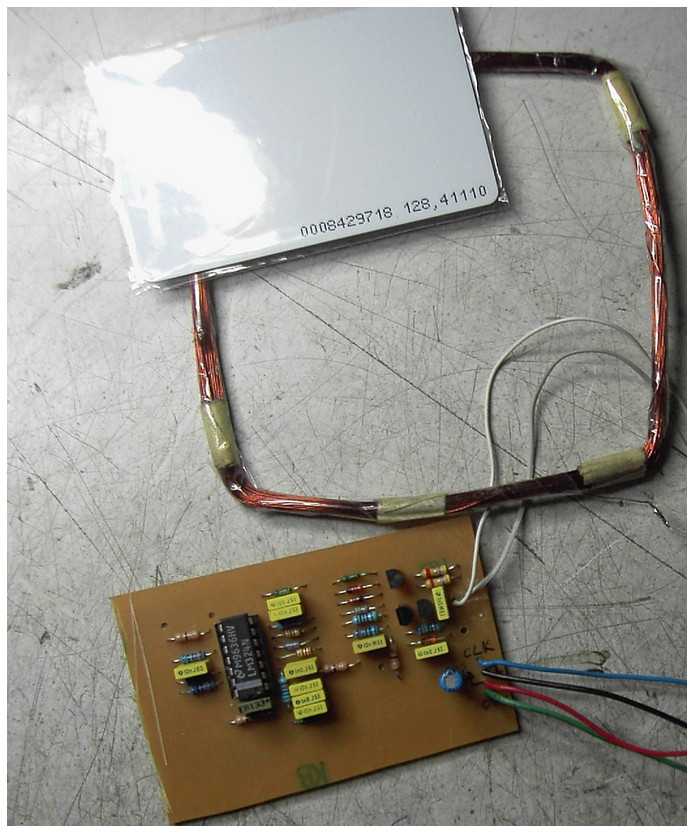
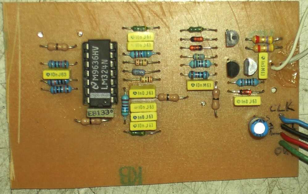
Finished PCB:
I am going to cover the digital section, that is the decoding part of this signal, in an another post.
One little hint; it is Manchester coding!
Until then, feel free to comment and share.
http://playground.arduino.cc/Main/DIYRFIDReader
http://playground.arduino.cc/uploads/Main/FSK-RFID-reader-v2.png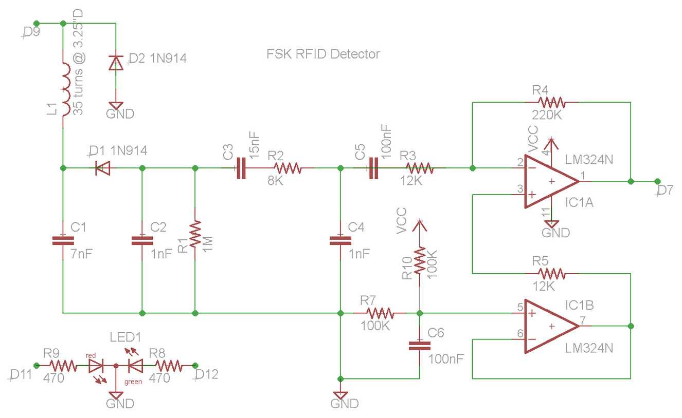
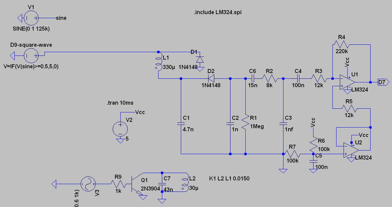
RFID Reader 线路图收集,布布扣,bubuko.com
原文:http://www.cnblogs.com/shangdawei/p/3729375.html