The present disclosure relates generally to integrated circuits, such as field programmable gate arrays (FPGAs). More particularly, the present disclosure relates to compilation of programmable logic on in an integrated circuit (e.g., an FPGA).
This section is intended to introduce the reader to various aspects of art. This discussion is believed to be helpful in providing the reader with background information to facilitate a better understanding of the various aspects of the present disclosure. Accordingly, it should be understood that these statements are to be read in this light, and not as admissions of prior art.
Integrated circuits (ICs) take a variety of forms. For instance, field programmable gate arrays (FPGAs) are integrated circuits that are intended as relatively general-purpose devices. FPGAs may include logic that may be programmed (e.g., configured) after manufacturing to provide any desired functionality that the FPGA is designed to support. Thus, FPGAs contain programmable logic, or logic blocks, that may be configured to perform a variety of functions on the FPGAs, according to a designer‘s design. Additionally, FPGAs may include input/output (I/O) logic, as well as high-speed communication circuitry. For instance, the high-speed communication circuitry may support various communication protocols and may include high-speed transceiver channels through which the FPGA may transmit serial data to and/or receive serial data from circuitry that is external to the FPGA.
In ICs such as FPGAs, the programmable logic is typically configured using low level programming languages such as VHDL or Verilog. Unfortunately, these low level programming languages may provide a low level of abstraction and, thus, may provide a development barrier for programmable logic designers. Higher level programming languages, such as Open CL have become useful for enabling more ease in programmable logic design. The higher level programs are used to generate code corresponding to the low level programming languages. Unfortunately, the conversion from higher level programming languages to low level programming languages oftentimes utilizes a substantial amount of time and processing power. In fact, the compile times for such conversions may oftentimes take many hours or even days to complete, causing a decrease in designer productivity.
Present embodiments relate to systems, methods, and devices for improving the compile time of Open CL programs through a multi-compile approach. In particular, the present embodiments may provide an Open CL compiler that provides both an initial thorough compile and an incremental compile. The initial compile generates a programming kernel that includes hardware descriptions for the programmable logic of the IC. From time to time, programmable logic designers may implement design changes. When these design changes occur, the compiler, through the incremental compile, may make changes to instructions implemented by the programming kernel without modifying the hardware descriptions, thus rendering the design changes in a far less time than compilation methods requiring generation of the hardware descriptions each time a design change occurs.
As discussed in further detail below, embodiments of the present disclosure relate generally to efficient compiling in an Open CL compiler. Traditionally, compilation in an Open CL compiler consists of a time and resource intensive cycle to generate hardware components needed to implement Open CL programs. Unfortunately, this cycle oftentimes takes many hours or even days to complete, causing an unsatisfactory experience for the programmable logic designers compiling high level code into low level instructions on the integrated circuit (IC). Traditionally, every change made to the high level code necessitated an additional time-intensive compile. The techniques discussed herein provide a two-level compile scheme that may provide more time-efficient compilations. The first level, an initial compile, generates a programming kernel that may include hardware descriptions to implement on programmable logic of the IC based upon the high level program provided by the programmable logic designers. The second level, or secondary compile, is useful for subsequent changes made to the high level program. The secondary compile utilizes a modified instruction set that may be implemented on the hardware generated in the initial compile to implement the subsequent changes. By merely modifying the instruction set without modifying the hardware definitions, subsequent compile times may be drastically reduced because the secondary compile may remove the time-intensive step of generating hardware for the programmable logic.
With the foregoing in mind, FIG. 1 is an exemplary block diagram of an Open CL compile path?10, illustrating the path of a high-level program implemented as low-level code on programmable logic of an integrated circuit (IC), such as a field programmable gate array (FPGA).
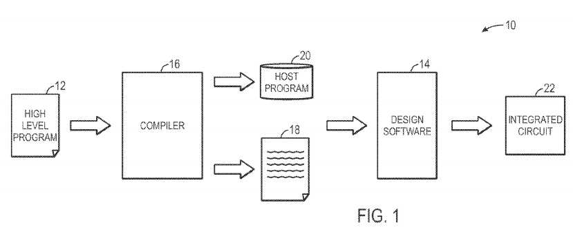
As illustrated, the Open CL compile path?10?begins with a high level program?12. The high level program?12?may contain programmable logic implemented by a logic designer. The programmable logic may be computer-readable instructions, written in a high level language, such as an Open CL programming language (e.g., the C++ programming language), which enables the logic designer to more efficiently and easily provide programming instructions to implement a set of programmable logic for an integrated circuit (IC) without a need for low level computer programming skills (e.g., Verilog or VHDL programming skills). Because Open CL is quite similar to other high level programming languages, such as C++, designers of programmable logic familiar with such programming languages may have a reduced learning curve than designers that are required to learn unfamiliar low level programming languages to implement new functionalities into the IC.
However, IC design software?14, such as Quartus II by Altera?, typically operates by using low level code instead of high level programming language instructions. Thus, a compiler?16, such as an OpenCL compiler, may be useful to interpret the high level program?12?to generate an intermediate low level code?18?and/or a host program?20?that provides implementation instructions for the low level code?18. The low level code?18?may be programming code, written in a hardware description language (HDL), such as a Verilog. The low level code?18?may define a grouping of hardware component logic useful for implementing the high level program?12?on the IC. The design software?14?may then interpret the low level code?18?to generate the programmable logic that includes hardware components necessary for implementation of the low level code?18. Once the design software?14, has generated the appropriate programmable logic, the programmable logic is implemented on the IC?22?(e.g., an FPGA).
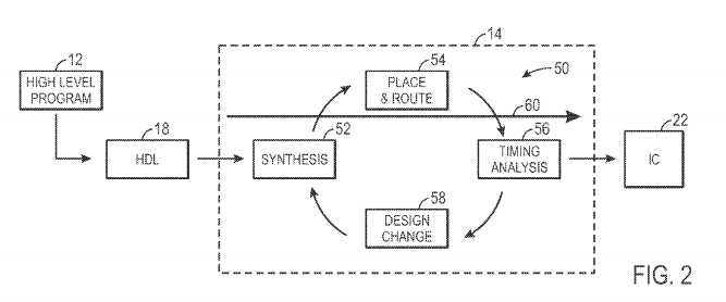
Unfortunately, as discussed above, the generation of programmable logic that includes a definition of the hardware components necessary for implementation of the low level code?18?is oftentimes a very time-intensive process. In fact, the process may take many hours or days to generate such suitable programmable logic. To provide a more detailed understanding of this time-intensive process, FIG. 2 illustrates an exemplary hardware component generation cycle useful for determining the hardware definition for programmable logic on an IC. As discussed above, the logic designer may implement a high level program?12?that is converted by a compiler into an HDL low level code?18. Design software?14?may interpret the low level code18?and generate the appropriate programming logic for implementation on the IC?22. To generate the programming logic, the design software?14?may utilize a computation and time intensive timing closure cycle?50. The timing closure cycle?50?may include synthesis?52, placement and routing?54, a timing analysis?56, and/or design change?58. The synthesis?52?includes determining a potential list of hardware components to be implemented on programmable logic of the IC, such that the HDL program may be executed on the IC. During the place and route?54, the design software?14?attempts to efficiently place the hardware components and route signals determined during the synthesis, such that storage and speed of the hardware components is efficient, such that the maximum operating frequency (Fmax) may be increased. During the timing analysis?56, the design software?14?determines if the Fmax for the placed and routed hardware elements and signals provides an Fmax that is within timing parameters specified by a programmable logic designer or the design software?14. If the placed and routed hardware elements and signals do not conform to the timing parameters, and the design software?14?implements a design change?58, modifying the programming logic to include a different set of hardware components. The synthesis?52?is repeated, utilizing a different set of hardware components and/or placement and routing configurations. The timing closure cycle?50?is repeated until the placed and routed hardware components and signals conform to the timing parameters. Unfortunately, the timing closure cycle?50?may need to be repeated numerous times to find an efficient solution to enable execution of the high level program?12, thus creating a large cycle time?60. Because the cycle time?60?may take quite some time, it may cause an unsatisfactory user experience for the programmable logic designer. Further, without the subsequent compile described herein, each time the programmable logic designer modifies the high level program?12, the design software?14?re-executes the time intensive timing closure cycle?50, repeating the time-intensive compile time.
To enhance the user experience, a two-level compile scheme may be implemented. The first-level or initial compile may be useful for generating hardware components to be implemented on the IC and the second-level or secondary compile may be useful for exploiting the hardware components of the initial compile to implement any changes made to the high level program?12?(or the low level code?18). FIGS. 3-8 are provided to more clearly illustrate the initial and secondary compile processes along with various scenarios that may be encountered when utilizing these compile processes.
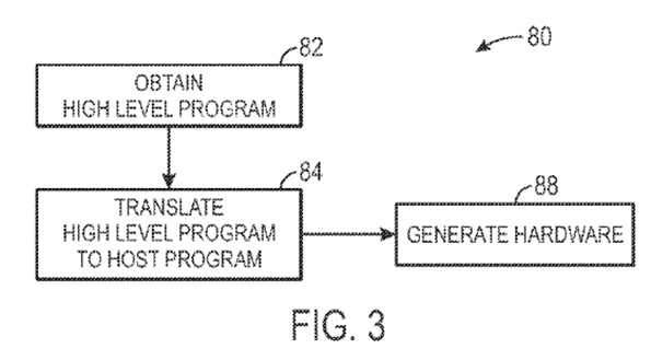
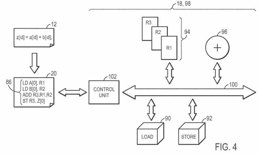
As discussed above, the two-level compile scheme may provide an initial compile that generates hardware components useful for implementation of a high level program?14. FIG. 3 is an exemplary flowchart illustrating an initial compile process?80. FIG. 4 is an exemplary block diagram providing an example of an initial compile process?80?for a high level program?12?that includes simple integer math.
As illustrated in FIG. 3, the initial compile?80?may begin by obtaining the high level program?12?(block?82). In the example of FIG. 4, the high level program includes a simple integer addition, storing the sum of a and b in z. The compiler?16?may translate the high level program?12?into a host program20?(block?84). As illustrated in FIG. 4, the host program?20?may include a low level instruction stream?86?that is a translation from the high level program12?into a low level host program?20?that may be implemented by the low level code?18. As illustrated, z[id]=a[id]+b[id] translates to load functions that load A[0] and B[0] into registers R1?and R2, respectively. An add function stores the summation of registers R1?and R2?in R3. A store function stores the value in register R3?in Z[0]. After the low level instruction stream?86?is generated, the design software?14?or the compiler?16?may generate the hardware (e.g., the low level code?18) necessary to implement the low level instruction stream?86?(block?88). For example, as illustrated in FIG. 4, because the instruction stream?86?includes load units?90, store units?92, registers?94?(e.g., R1, R2, and R3), and an addition functional unit?96, the hardware definition?98, defined by the low level code?18, includes each of these components generated on a data path?100?for use in the programmable logic of the IC?22. Further, a control unit?102?(e.g., a state machine) may control the data path?100?by instructing the components connected to the data path?100?(e.g., the load units?90?and the store units?92) based upon the low level instruction stream?86, such that the low level instruction stream?86may be implemented. As will be discussed in more detail below, the hardware definition?98?is not limited to hardware components useful for the implementation of the current low level instruction stream?86. Indeed, as will be discussed in more detail below, the hardware definition?98?may include many components that are not utilized in the programming logic provided to the compiler?16.
In generating the hardware, the initial compile will process the components according to the timing closure cycle?50. Thus, the initial cycle may utilize hours and/or days to complete. However, as will be discussed in more detail below, the initial compile may generate hardware definition?98?that, in an unmodified state, are still useful for certain modifications made to the high level program?12?and/or the low level instruction stream?86?without utilizing an additional initial compile to re-generate the hardware definition?98.
The secondary compile may be useful to implement modifications made to the high level program?12?and/or the low level instruction stream?86?without regeneration of hardware components through an initial compile. FIG.5 illustrates an exemplary secondary compile process?110?and FIGS. 6-8 illustrate various scenarios that may be encountered after the high level program?12?is modified. As illustrated in FIG. 5, the secondary compile process?110?may be initiated when a logic designer modifies the high level program?12?(block?112). A poll is completed to determine whether existing hardware has been generated for the high level program?12?(block?114). In alternative embodiments, the designer may simply choose an option to compile using a secondary compile, such that the design software?14?may safely assume that hardware generation has previously occurred. If no hardware has been generated previously, the initial compile process?80?is executed. However, if a previous hardware generation has occurred, the hardware definition?98is obtained (block?116). The design software?14?and/or the compiler?16?determines whether the high level program modification may be implemented by the current hardware definition?98?(block?118). When the modification cannot be implemented using the existing hardware definition?98, the initial compile process?80?is executed, generating a new hardware definition?98?based upon the modified high level program?112. However, in certain embodiments, when the current hardware definition?98?is sufficient to implement the modified high level program?112, a secondary poll (block?120) may be implemented. The secondary poll determines whether implementing the modification using the current hardware definition?98?would fit within pre-defined efficiency boundaries set in the design software?14?or elsewhere. For example, in some embodiments, the design software?14?may determine a difference between the throughput of a critical path using the original hardware versus the throughput of a critical path that would result if a full recompile were performed. If the throughput difference is within Fmax noise, then the design software may determine that the efficiency is within efficiency bounds. However, if the different is not within Fmax noise, then the design software may determine that the efficiency is not within the efficiency bounds.
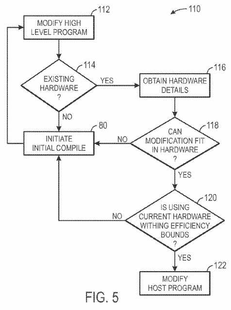
If implementing the modification using the current hardware definition?98?would result in unacceptable efficiency (e.g., as defined by the efficiency boundaries), the initial compile process?80?is initiated, thus generating new hardware components based upon the modified high level program?112. However, when the modifications can be implemented within the efficiency bounds utilizing the same hardware definition?98, the secondary compile ends by modifying the low level instruction stream?86?to implement the modifications on the current hardware definition?98?(block?122).
In some embodiments, rather than automatically progressing to block?122, the designer may be provided a prompt allowing the designer to specify whether the hardware definition?98?should be regenerated through a subsequent initial compile or whether the current hardware should be utilized despite the efficiency of the programmable logic not falling within the efficiency boundaries. Such choice enables the designer to guide the process by selecting a tradeoff of a potentially lengthy compile time or a potentially less efficient design, thus catering to the designer‘s preferences.
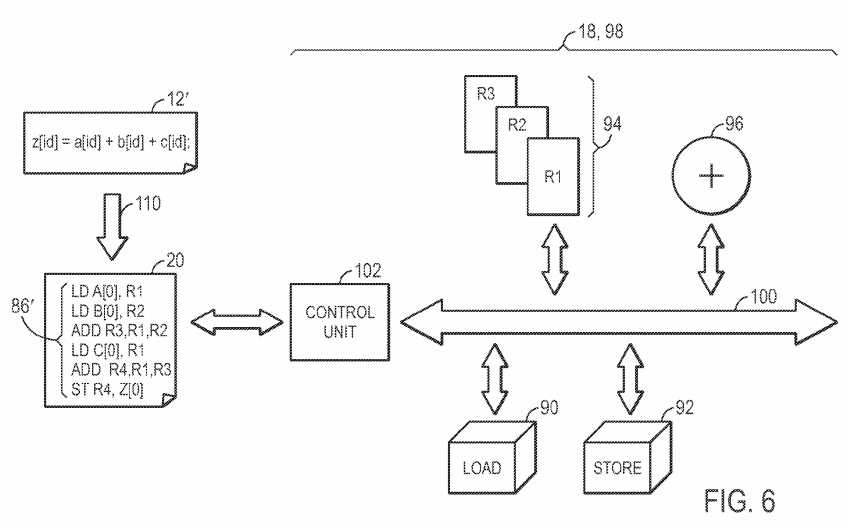
FIG. 6 illustrates an exemplary high level program?12′ that includes a simple modification from the high level program?12?of FIG. 4 that may be implemented by the original hardware definition?98?of FIG. 4. As illustrated, in the provided example, the logic designer has modified the original high level program?12?by adding an additional variable c[id] to the summation stored in z[id]. The high level program is translated into a low level instruction stream?86′. As illustrated, the modifications from low level instruction stream?86?to low level instruction stream?86′ are fairly minor, utilizing one additional load and one additional addition instruction. Thus, the design software?14?may determine that the modification may be implemented with the current hardware definition?98?and that such implementation would fall within the predefined efficiency boundaries. Thus, to implement the change, the implemented low level instruction stream?86?may be modified to incorporate the changes of low level instruction stream?86′. Thus, the modifications of high level program?12′ may be implemented without the need for an initial compile?80, thus skipping the time-intensive timing closure cycle?50.
In some instances, modifications made to the high level program?12?may be implemented using the current hardware definition?98, but such implementation may be unacceptable due to inefficiency of the prescribed implementation. For example, FIG. 7 illustrates an exemplary high level program?12″ that provides a more complex low level instruction stream?86″ than the low level instruction stream?86′ of FIG. 6. In the provided example, the designer has modified the high level program?12?to multiple instead of sum a[id] and b[id]. As illustrated in FIG. 4, the current hardware definition?98does not include a multiplication functional unit. However, through the secondary compile process?110, the design software?14?may recognize an alternative set of low level instructions that may be implemented using the current hardware definition?98. For example, as illustrated, the low level instruction stream?86″ includes an addition loop, used as a substitution for a multiplication functional unit. Thus, the modification may be implemented without change to the current hardware definition?98.
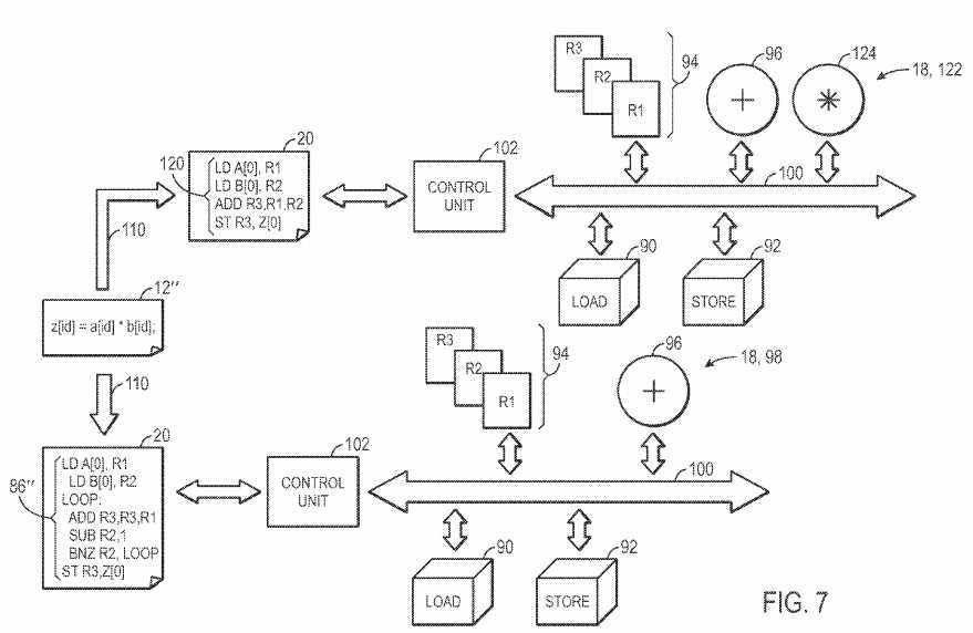
However, the loop may add significant inefficiency to the implementation or the pre-defined efficiency bounds may be strict, and thus the implementation may not fall within pre-defined efficiency boundaries. Thus, an initial compile process?80?may be executed, such that a new low level instruction stream120?with a new hardware definition?122?having a multiplication functional unit?124?are implemented. By generating a new low level instruction stream120?and the new hardware definition?122, the programmable logic may be more efficient and conform to the efficiencies standards.
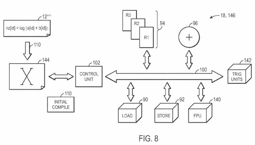
In certain situations, the current hardware definition?98?cannot implement the modifications to the high level program?12?made by the logic designer. FIG. 8 provides one such example. As illustrated, the high level program?12?has been modified to a high level program?12′″ that uses a logarithm function, and thus utilizes floating point functional units?140?as well as trigonometry functional units?142. Because the current hardware definition?98does not include floating point functional units?140?or trigonometry units?142, the design software cannot translate the high level program?12′″ into a low level instruction stream that may be implemented by the current hardware definition?98?(as is illustrated by the void low level instruction stream?144). Thus, a full initial compile?110?is initiated, generating the hardware definition?146?that includes the floating point units?140?and the trigonometry units142.
As illustrated by the examples provided by FIGS. 6-8, hardware generation may be avoided when modifying a high level program?12?if a secondary compile can be used to create an implementation using the existing hardware definition and the implementation falls within acceptable efficiency boundaries. Keeping this in mind, it may be beneficial to incorporate additional considerations when completing an initial compile, such that the number of initial compiles needed for modifications to the high level program?12?may be reduced.
Many considerations and efficiencies may increase the Fmax of a resultant implementation and/or reduce the number of initial compiles that a programmable logic designer may encounter. For example, the length and/or complexity of the data path?100?may directly impact the throughput, and thus the Fmax, of an implementation. Further, the number of available programming kernels may affect the throughput of the implementation. Also, by adding flexibility to the kernels and/or enabling the selective initial compilation of specific kernels, the number and/or time length of the initial compiles may be greatly reduced. The compiler?16?may take into account these considerations when deciding how to generate hardware and implement the high level program?12.
i. Data Path Trade-Offs
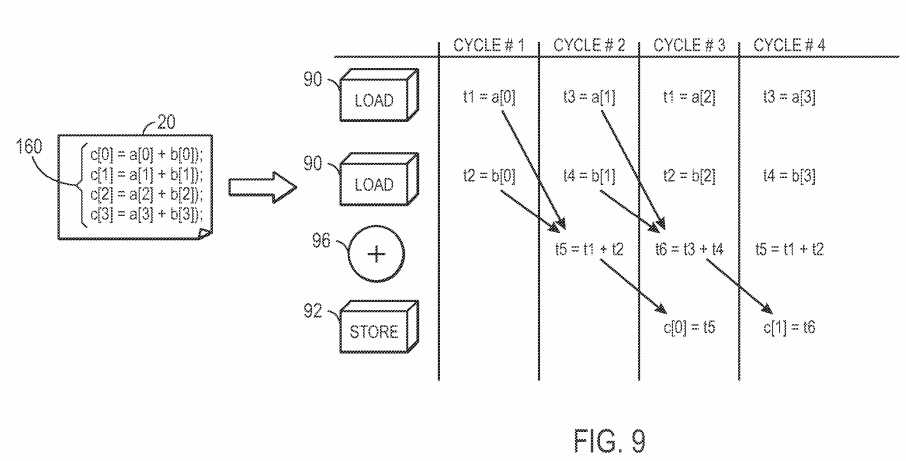
OpenCL enables more ease in the execution of instructions in parallel, thus increasing programmable logic efficiency. For example, FIG. 9 illustrates multiple OpenCL threads?160?(e.g., instructions in a high level program?12) that may be executed in parallel. As illustrated, the OpenCL threads?160include multiple summation computational threads. As previously discussed with regards to FIG. 4, addition threads may be implemented through use of load units?90, store units?92, and addition functional unit?96. As illustrated in the example of FIG. 9, in a first clock cycle, the load units may load a[0] and b[0]. In the second clock cycle, the addition functional unit?96?may be used to sum the loaded values a[0] and b[0] and the second thread may be initiated, loading a[1] and b[1]. In the third clock cycle, the summation of a[0] and b[0] may be stored in c[0], completing the execution of the first thread. Additionally, the values loaded in the previous cycle may be added using the addition functional unit?96. Further, values a[2] and b[2] may be loaded by the load units?96, thus initiating the third thread. In the fourth cycle, the summation of the third cycle is stored in c[1], thus completing the second thread of execution. Further, the loaded values from the third cycle are added by the addition functional unit?96?and values a[3] and b[3] are loaded by the load units?90, thus initiating the fourth thread. This cycle may continue, until each of the threads have been executed to completion. As may be seen by this example, parallel execution may provide great efficiency by keeping the maximum number of functional units busy at every clock cycle. Thus, the compiler may include considerations to efficiently ensure that threads may be executed in parallel.
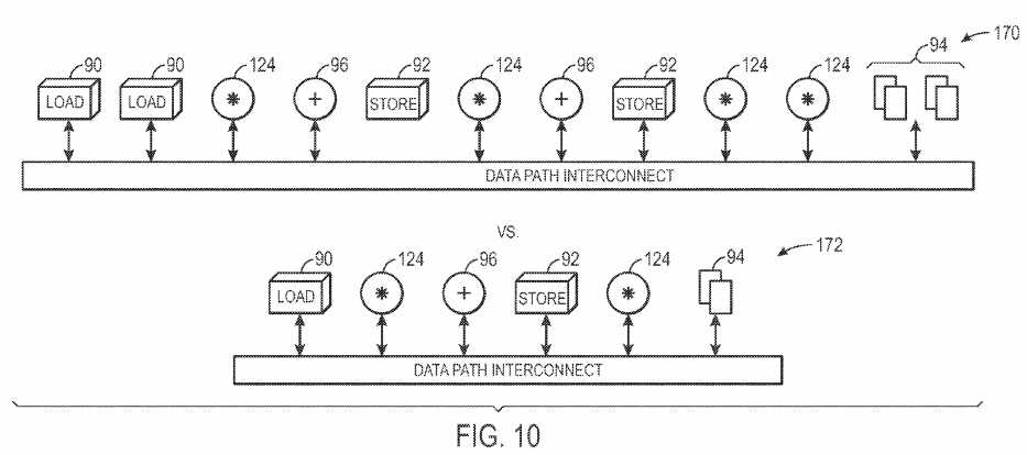
The size of the data path may directly affect the throughput of an implemented thread. While the data path may be minimized by incorporating only one functional unit for each fundamental operation of a thread, under certain situations, it may be beneficial to add additional functional units to the data path. FIG. 10 illustrates an exemplary comparison of two example data paths?170?and?172. Data path?170?is a complex data path with numerous functional units, whereas data path?172?is a more simplistic data path with a reduced number of functional units. For example, complex data path?170includes twice as many load units?90, store units?92, registers?94, addition functional units?96, and multiplication functional units?124?as the more simplistic data path?172. There are pros and cons to implementing complex data paths?170?versus more simplistic data paths?172. Depending on specific priorities, either may be chosen over the other. For example, there may be two over-arching goals to consider when determining the complexity of the data path. First, complex data paths?170?may be more efficient by providing an ability to execute threads in the fewest cycles possible, while supporting many overlapping parallel threads. For example, due to the increased number of functional units, many threads of computation may be added in parallel without the data path becoming saturated. Thus, there may be increased efficiency for a high number of threads in the high level program?12. However, a second goal in selecting an appropriate data path is to reduce the area consumed in the programmable logic of the IC. As optional functional units are added to the data path, the amount of area needed to store the data path may grow quadratically. However, such a data path may enable more threads?106?to be added without saturating the data path, thus generating more throughput. Less complex data paths may be duplicated to increase throughput within the system. With the foregoing in mind, the compiler?16?may analyze the tradeoff between the area consumed by the programmable logic and the computation throughput to determine whether a complex data path?170?or a more simplistic data path?172?should be used.
In some instances, the compiler?16?may use the evaluation equation:

to evaluate the efficiency of the data path size. For example, the compiler?16?may start with the complex data path?172?and evaluate using the evaluation algorithm. The compiler?16?may iteratively remove one or more functional units (e.g., a multiplication functional unit?124) and re-evaluate using the evaluation equation and record the evaluation results. Thus, the compiler?16?may determine the solution with the best balanced results and implement the corresponding data path size.?
ii. Multi-Kernel Optimization
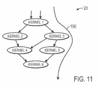
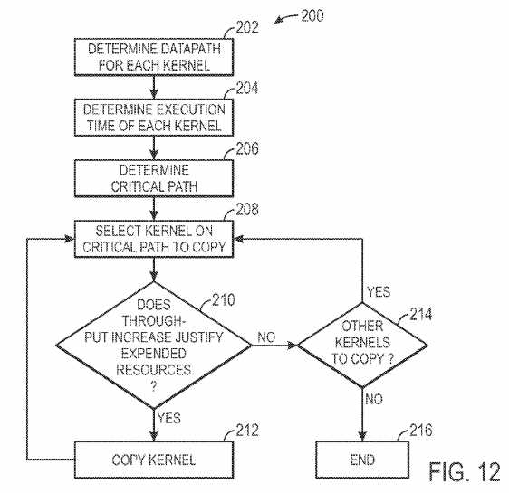
Having now discussed optimization of the data path and low level instruction stream for a single Open CL kernel, the discussion now turns to a consideration of a multi-kernel program implementation. FIG. 11 is an exemplary call graph illustrating a host program?20?that utilizes multiple kernels in its execution. As illustrated, the host program?20?may define a call path of the multiple kernels. Line?190?represents the critical path (e.g., the most time-intensive path) called by the host program?20. Because the critical path?190?is the most time-intensive path called by the host program?20, providing added efficiency to the critical path?190?may likely have more impact to overall performance than increasing the efficiency of other call paths. FIG. 12 is an exemplary flow chart illustrating a process?200?for increasing the efficiency of a critical path?190, in accordance with an embodiment. The compiler16?or other computer processing device may determine the kernels called by host program?20?and estimate the data path for each kernel (block?202). The execution time of each kernel may be calculated (block?204) by determining the data path parallelism, or number of parallel overlapping threads, and the cycles per thread for each kernel. Knowing the execution time for each kernel, the execution times for each kernel in the call path may be summed to determine the critical path (block?206). For example, in the example of FIG. 11, one call path timing would be calculated by summing the execution times for kernels?1,?2,?4, and?6. Another call path timing would be calculated by summing the execution times for kernels?1,?3,?4, and?6. Yet another call path timing would be calculated by summing the execution times for kernels?1,?3,?5, and?6. The call path with the largest timing (e.g., the path with kernels?1,?3,?5, and?6?in our example) would be determined to be the critical path. It is important to note that while the current example does not illustrate a looped call path, timings for such paths may still be calculated by obtaining profiling information to understand a number of times the loop may occur, thus adding the timing of the kernels in the loop to the timing summation an appropriate number of times. Once the critical path?190?is determined, any kernel on the critical path?190?(e.g., kernel?1,?3,?5, and/or?6) may be selected for copying (block?208). As discussed above, by duplicating a kernel, the throughput may be increased. By increasing the throughput on the critical path, the efficiency of the overall system may be increased. The compiler?16may evaluate whether implementing an additional copy of the selected kernel would be beneficial (block?210). For example, the compiler?16?may determine the amount of resources necessary to implement a new copy of the selected kernel as well as the efficiency gain by implementing the new copy of the selected kernel and decide whether the new copy should be implemented. If the new copy should be implemented, the kernel is copied (block?212) and the kernel selection (block?208) is repeated, selecting either the same kernel that was copied in block?212?or a different kernel on the critical path?190. If, however, the compiler?16?determines that it is not beneficial to implement a copy of the selected kernel, the compiler?16?may determine whether there is another kernel that may be copied (block?214). If there is another kernel that may be copied, the kernel selection (block?208) is repeated, selecting a different kernel. The process?200?may continue until certain bypass metrics are met or when no other kernels are on the critical path?190. For example, when no further kernels on the critical path?190?are available to be copied, the process?200?is ended (block?216). Further, bypass metrics such as: exceeding a pre-determined number of kernel copy iterations, the exhaustion of IC resources beyond a threshold value, or determining that throughput metrics have not increased for a certain number of iterations may cause the process?200?to end (block?216).
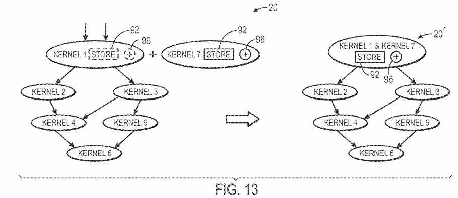
When adding new kernels to the host program?20, it may be beneficial to determine whether the new kernel can fit within existing kernels. For example, FIG. 13 illustrates an exemplary scenario where a new kernel, kernel?7?is added to the host program?20. When the compiler?16?determines that a new kernel should be added, the compiler?16?may detect whether the functional units of kernel?8?may be found in an already existing kernel. For example, if one kernel has unused functional units that are the functional units utilized in the new kernel, the existing kernel may be modified to implement the new kernel functionalities. For example, if kernel?7?consists of a store functional unit?92?and an add functional unit?96, the compiler?16?may look for unused store functional units?92?and add functional units?96. As illustrated in FIG. 13, kernel?1?may include an unused store functional unit?92?and an unused functional unit?96. Because an existing kernel includes the unused functional units necessary to implement kernel?7, kernel?1?may be modified to also perform the functions of kernel?7, as illustrated in resultant host program?20′.
In some embodiments, the compiler?16?may detect unused functional units across multiple kernels and may utilize the unused functional units to generate new kernels. For example, FIG. 14 provides one example of kernel?7′s functionality being implemented in part on kernel?1?and in part on kernel3. As discussed above with regards to FIG. 13, kernel?7?utilizes a store functional unit?92?and an addition functional unit?96. In the depicted example, kernel?1?includes an unused store functional unit?92?and kernel?3?includes an unused addition functional unit?96. As illustrated, the compiler?16?may modify kernels?1?and?3?to perform portions of the functionality of kernel?7?(e.g., portion A of kernel?7?in kernel?1?and portion b of kernel?7?in kernel?3). Because the new kernel‘s functionalities may be implemented through existing kernels, no new kernels need be generated, and thus, the compile time may be greatly decreased.
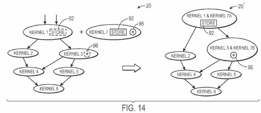
While the current example illustrates all of the functionalities of the new kernel being satisfied by unused hardware in existing kernels, in some embodiments, only a portion of functionality may be satisfied by unused functional units of the existing kernels, thus causing a new kernel to be generated. Despite generation of the new kernel, it may be beneficial to utilize at least some of the unused functional units of the existing kernels. For example, such a scheme may make the hardware generation in a subsequent compile less complex and therefore less time consuming. Thus, even when the compiler?16?determines that a new kernel should be created, the compiler?16?may still utilize unused functional units of the existing kernels.
iii. Compiler Flexibility
During the two-level compile process, the design software?14?may be enabled to receive user guidance from the programmable logic designers, thus enabling the compiler?16?to alleviate excessive initial compiles based upon designer input. For example, when a new project begins, the design software14?may prompt the programmable logic designer for an intended vertical market that the programmable logic will be designed for. A vertical market may be a business that engages in trade based on specific and specialized needs. For example, vertical market parameters provided to the design software14?may include financial services and/or the oil & gas industry. Based upon the vertical market provided before an initial compilation, the compiler?16?or design software?14?may determine a set of useful functional units to add, regardless of whether current kernels will utilize the functional units. Such unused functional units may increase the hardware flexibility of the compiled programmable logic, helping to reduce subsequent initial compiles necessary to add additional functional units. For example, financial service vertical markets may utilize many of the trigonometry functional units as well as floating point functional units such as logarithm, square root, and double precision operational units. In contrast, oil & gas operations may frequently utilize a vastly different subset of functional units. If a designer guides the compiler?16?or the design software?14?to specifically compile the programmable logic for financial services, the compiler?16?or design software?14?may include an expansion set of functional units that is particularly geared towards financial services (e.g. the trigonometry and/or floating point functional units). In certain embodiments, one floating point functional unit may be incorporated into each kernel when there is sufficient programmable logic storage area to contain the additional functional units. Thus, as described above, the unused functional units may reduce subsequent initial compiles by enabling increased flexibility in generated kernels by providing of an expansion set of functional units to be used by newly created kernels.
However, this added flexibility may increase the amount of programmable storage space that is utilized by the programmable logic, and thus may be undesirable for some programmable logic designs. Thus, the designer may provide guidance (e.g., via an input to the design software?14) to turn off this flexibility feature, so that programmable logic space is conserved. For example, when a programmable logic design is more or less complete, with relatively little change of substantial future modifications, the designer may desire to reduce the storage area of the individual kernels, and instead replicate kernels, as discussed above, to increase throughput and, ultimately, the performance of the entire programmable logic design. Thus, by enabling the designer to turn off the flexibility function, the design may be more accurately customized, based upon the designer‘s guidance.
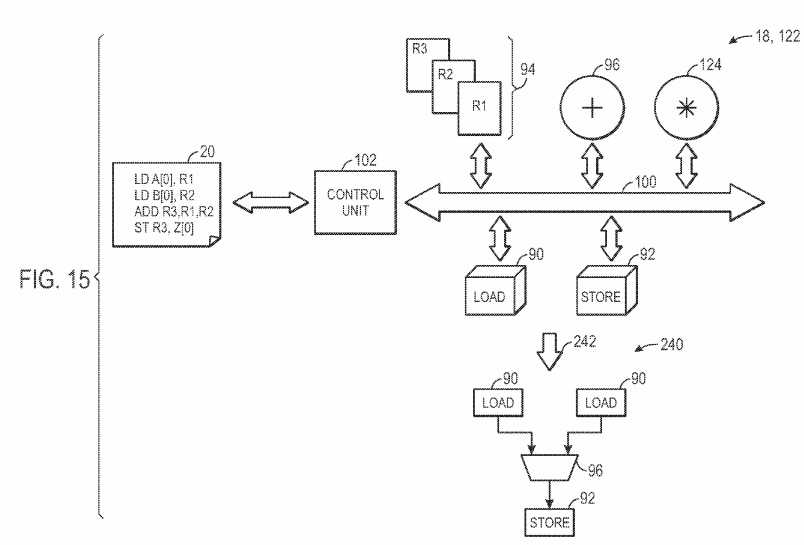
An additional compiler flexibility that may be implemented in certain embodiments, includes an ability of the designer to increase efficiency by providing guidance to selectively migrate certain kernels from a data path/programmable control implementation to a more efficient hardware pipeline implementation. Such functionality may be desired, for example, near the end of a design cycle, where efficiency may be more of a focus than functional growth. FIG. 15 illustrates an exemplary kernel implemented as an instruction set and data path that is migrated to a hardware pipeline, based upon guidance from the designer. As illustrated, the kernel may be implemented with programmability through use of the control unit?102?and the host program20. However, when a designer desires to provide increased efficiency of the kernel, the designer may guide the compiler?16?or design software?14?to migrate the kernel to a fixed hardware pipeline, removing all programmability of the kernel. In the example of FIG. 15, the programmable kernel includes load functional units?90, store functional units?92, registers?94, an addition functional unit?96, and a multiplication functional unit?124?coupled via the data path?100. As illustrated, the host program?20?provides instructions to the control unit?102?to utilize the load unit?90, the addition functional unit?96, and the store unit?92. When the designer desires an efficiency tradeoff (e.g., increase Fmax) over a functional flexibility tradeoff (e.g., programmability), the designer may provide an indication to the compiler?16?or design software?14?such that the programmable kernel?122?may be migrated to a non-programmable hardware pipeline?240. Upon receiving this indication, the compiler?16?or design software?14?may convert the programmable kernel?122into the non-programmable hardware pipeline?240. In the example of FIG. 15, the design software?14?has converted the programmable kernel?122?into a non-programmable hardware pipeline?240, as indicated by arrow?242. Because the host program?20?utilizes two calls to the load unit?90, a call of the addition functional unit?96, and the store unit?92, the non-programmable hardware pipeline?240?includes two load units?90, an addition functional unit?96, and a store unit?92. As may be observed from this example, the control unit?102?is not present because there are no programming instructions to be interpreted to control the non-programmable hardware pipeline?240. Further, because the multiplication unit?124?is not utilized by the host program?20, it is not incorporated into the hardware pipeline?240. By removing the programmability of the kernel, the functional flexibility of the kernel may be greatly reduced. However, such modification may result in a substantial efficiency improvement (e.g., reduced amount of programmable logic area utilized and/or increased Fmax). For example, in some embodiments, by converting the kernel of FIG. 15 into a non-programmable hardware pipeline?240?for simple addition, the Fmax performance may increase by three times that of the programmable kernel.
Another efficiency that may be enabled by the two-level compile process is selective partitioning of kernels such that kernels of a common type may be compiled while kernels of an alternative type are not compiled. FIG. 16 illustrates exemplary programmable logic?260?with design partitions?262. The design partitions?262?may be enabled to store one or more kernels of a similar type (e.g., with common functional units). For example, kernels?264?are stored in one partition?262, kernels?266?are stored in a second partition?262, and kernels?268?are stored in a third partition?262. By storing similar typed kernels in the design partitions?262, the design software?16?may be enabled to execute initial and/or secondary compiles for only a sub-set of kernels contained within a particular design partition?262. Further, the designer may provide guidance to convert kernels within a particular partition to a non-programmable hardware pipeline for performance enhancements.
As previously discussed, the two-level compile process provided herein is useful to reduce the processing power and time to compile programmable logic for an IC, providing a more satisfactory design experience. Through guidance by the designer, the two-level compile process may be further enhanced for a particular design, enabling a compile experience that is uniquely geared towards the designer‘s project. Such customization may add flexibility to design, decrease compile time, and/or increase the performance of designer‘s program.
SRC=http://www.freepatentsonline.com/y2013/0346953.html
PatentTips - OpenCL compilation,布布扣,bubuko.com
PatentTips - OpenCL compilation
原文:http://www.cnblogs.com/coryxie/p/3839736.html